


PROBOTS - ABOUT US
Probots offers Electronics Engineering Services to get your product from concept to production. We provide the following services - Circuit Designing, PCB Designing, Embedded Firmware Development, etc. We have successfully designed 100+ products in IoT, AI & ML, Automation, Robotics, Industrial Monitoring, Generic Consumer Devices, and Medical Devices.
We help customers build their own design and prototypes by supplying electronic parts. We stock a wide range of parts that we use for manufacturing products. These products are carefully sourced from best manufacturers at bulk pricings and we pass on the benefits to our customers. We sell Arduino, Raspberry Pi, IoT Sensors, ESP32, STM32 Development Boards, Electronic Components, Prototyping Tools and Robotics Parts.
Buy Arduino, Raspberry Pi, NodeMCU ESP32, Electronic Components, Plastic Enclosures and much more at Probots - India’s Largest Engineering and DIY Store
As one of India’s biggest distributors of electronic and technological components for the Embedded Systems and Robotics, we offer more than 110,000 products at a unique price-performance ratio, with maximum availability and minimum delivery times. With our broad spectrum of electronic components we are the ideal partner for component purchasing. In our online shop electronics engineers will find ICs and microcontrollers, as well as LEDs and transistors. We also offer resistors, capacitors, and pin-and-socket connectors and relays. We have the right equipment for your workplace, including soldering stations and multimeters as well as and high-quality tools. In addition, our product spectrum includes a large selection of items from plastic enclosures accessories and HDMI cables, batteries and rechargeable batteries. Have a look at our large selection of accessories. When it comes to and as well as connectors and memory cards our emphasis is on top quality at very attractive prices. Try out our fast dispatch service and top customer support, and compare our prices: We are certain that you will soon be among our satisfied customers.
WHERE TO BUY ELECTRONIC COMPONENTS ONLINE IN INDIA?
Probots sells the following items online - Arduino, Raspberry Pi Development Boards, NodeMCU ESP8266, ESP32, Sensors Modules, Electronic Components, Plastic Enclosures for Electronics, SMPS Power Suppliers, Resistors, Capacitors, and a wide range of products. You can order online on our website and we will deliver throughout India within 1-15 days.
ONLINE SHOPPING MADE EASY AT PROBOTS
If you would like to experience the best of online shopping for Electronic Modules & Components in India, you are at the right place. Probots is the ultimate destination for Electronics & Robotics, being host to a wide array of merchandise including Arduino, Raspberry Pi, NodeMCU ESP32, Sensors, Motor Drivers, Power Suppliers, SMPS, Batteries, Electronic Components, etc. You can get every part for your next project online and stop worrying about sourcing components from multiple sources. We sell products only after careful selection among multiple vendors. You can shop online at Probots from the comfort of your home and get your favourites delivered right to your doorstep.
BEST ONLINE SHOPPING SITE IN INDIA FOR ELECTRONICS & ROBOTICS
Irrespective of your project - IoT, Robotics, Python, OpenCV, AI, ML, Embedded Electronics, Automation, etc you will find all required components at probots.co.in. You will realise that the sky is the limit when it comes to the parts used in these projects and you can purchase them online on our store.
- Plastic Enclosures
- Electronic Modules
- Electronics Components
- Tools & Prototyping
- Robotics
BUY PLASTIC ENCLOSURES FOR ELECTRONICS IN INDIA
Probots manufactures and retails 100+plastic boxes and cases for electronic circuits. No minimum order quantity, bulk discounts available for business purchase. We make enclosures boxes for sensor nodes, controllers, IoT Products, handheld devices, wearables, wall mount devices, etc.
Probots sells generic low cost effect enclosures, high quality premium IP65 Dust and Waterproof Enclosures, Enclosures with Transparent Lids, etc We have circuit enclosures boxes for all sizes - small, medium and large PCB boards. We also have Aluminium Enclosures, ABS enclosures, PVC Enclosures, Cabinets, Metal Boxes, etc. We also sell IP65 Waterproof PVC & Metal Cable Glands and Fan Filters
BUY Arduino Board Online India
Probots sells Arduino UNO, Arduino Mega, Arduino Nano, Arduino Pro, Mini, Micro, Lilypad, Due, and other development boards online in India. These boards come with Atmega328 and Atmega2560 and are great for learning electronics and programming. Order them online for your next robotics, electronic, IoT Project.
BUY Raspberry Pi Online India
Probots sells Raspberry Pi, Pico SBC (Single Board Computer), HDMI Displays, Raspberry Pi Starter Kit. We source them from official Distributors and offer the best quality development boards at lowest prices possible. We also sell a wide range of Raspberry Pi Accesories - Raspberry Pi Cameras & Lens, Heat sink Cases for Raspberry Pi, Raspberry Pi Sensors, Raspberry PI Power supplies, etc. Buy Raspberry Pi Online Now for your next Machine Vision Project, OpenCV Project, Image processing and recognition project!
Electronic Sensor Modules Online at Probots India
Buy Online Ultrasonic Sensors, Distance Sensors, Temperature Sensors, PIR Motion Sensors, ph Soil Sensors, Encoder Sensors, Magnetic Door Lock Sensors, Gas Sensors, Accelerometers & IMU Modules, Line Following Sensors, Force Flex Sensors, Current and Voltage Sensors, Flow Sensors, Light Sensors, Biometric Fingerprint Sensors, etc. We also have the latest electronic sensors for electronics and robotics like sound and voice sensors, Gesture Recognition SEnsors, Load Cell Weight Sensors, etc. These sensors can be used with Arduino, Raspberry Pi, NodeMCU, ESP32 and other microcontrollers. Use them in your next electronics project. Order them online now.
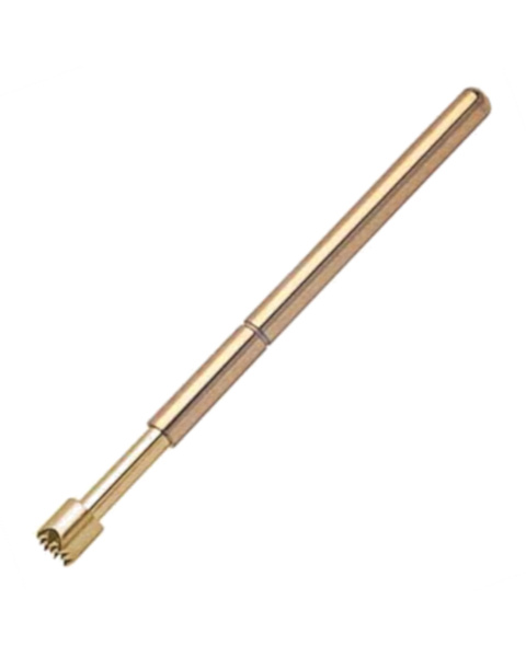
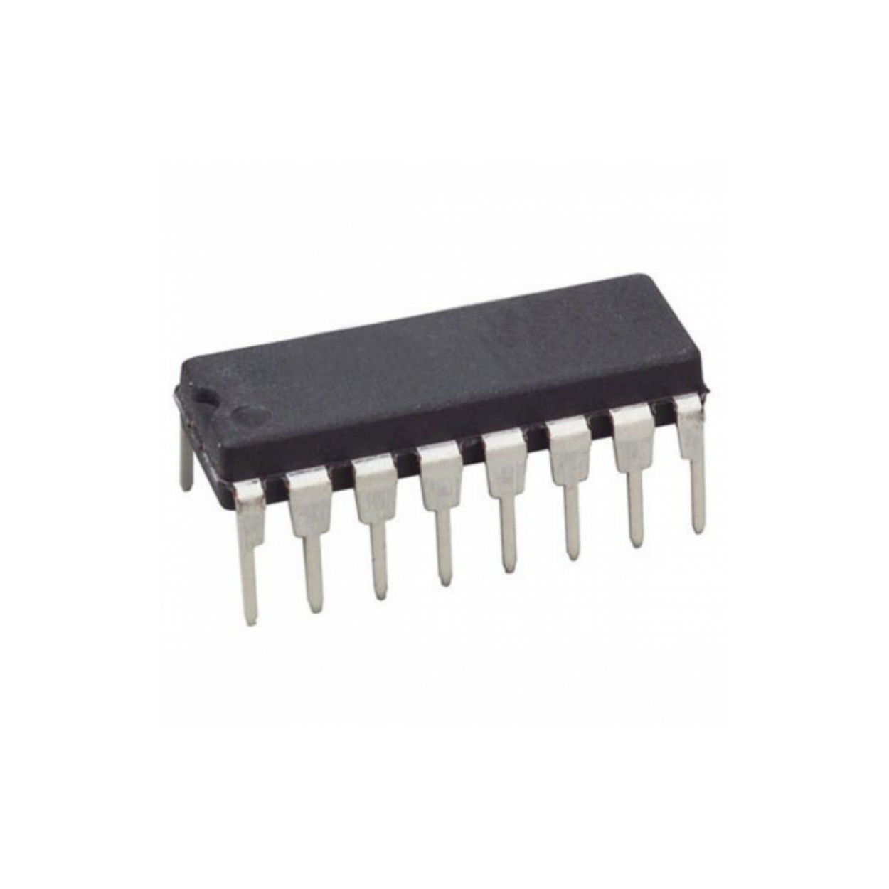
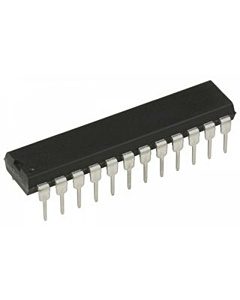
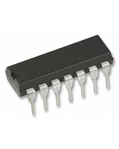
Best Online Store for buying Electronic Components
Bits and pieces that make your project work are always hard to find. Probots has 500+ electronic components like Microcontroller ICs, LEDs, Header Pins, Connectors, Crystal Oscillators, Cables, Buzzers, Transistors, Motor Driver ICs,
Voltage Regulator ICs, ZIF & DIP Sockets, LED Holders, Switches, Potentiometers, LCD Displays, ICs, Resistors, Batteries & Holders, Heatsinks, Capacitors, Relays, Diodes, Heat shrink tubes, LED Displays, DIP Switches, Resistor Arrays, 7 Segment Displays, LED Strips, etc Chekout our wide range of electronic components and order them online in India now.
AFFORDABLE PARTS AT YOUR FINGERTIPS
Probots is one of the unique online electronics shopping sites in India where components are accessible to all. Check out our new arrivals to view the latest microcontrollers, sensors and ICs in the market.
HISTORY OF PROBOTS
Becoming India’s no. 1 electronics destination is not an easy feat. Sincere efforts, digital enhancements and a team of dedicated personnel with an equally loyal customer base have made Proobts the onlie platform that it is today. The original B2C venture for electronics components was conceived in 2009 but transitioned into a full-fledged ecommerce giant within a span of just a few years. By 2012, Probots introduced 350 Indian and international brands to its platform, and this has only grown in number each passing year. Today Probots sits on top of the online electronics field with an astounding social media following, a loyalty program dedicated to its customers, and tempting, hard-to-say-no-to deals.
Probots Techno Solutions offers complete turn-key Embedded Electronics Design & Engineering Services. We can work on Product Specification through Prototyping, Proof of Concept to Production depending on individual client needs.
Probots is one of the top Electronics Design companies based out of Bangalore. We provide range of Embedded Engineering Services that include Circuit Designing, PCB Designing, Customised IoT Hardware, Embedded Firmware Development, Hardware Prototyping, Proof of Concepts & Electronic Manufacturing Services.
With close to 10 years of solid experience in Electronics Design, we have successfully completed 100s of complex Electronic Product Designs across a wide range of domains - Consumer Products, Industrial, Medical and Aerospace Industries. Our team has completed projects for Fortune 500 companies as well as start-ups using both traditional and cutting edge technologies.
Probots also offers consultancy, and testing services across the product and process development life cycle.
Our biggest strength is our agile team that utilises our core experience, to deliver quick turnarounds giving you faster time-to-market.